
We use cookies to improve the Bookmate website experience and our recommendations.
To learn more, please read our Cookie Policy.
To learn more, please read our Cookie Policy.
Accept All Cookies
Cookie Settings
Something went wrong. Try again.

Books
Read in our apps:
iOS
·Android
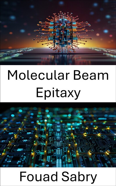
The world of Nanoelectronics is evolving rapidly, and understanding the cuttingedge technologies behind this field is essential for professionals, students, and enthusiasts alike. “Molecular Beam Epitaxy” is an indispensable resource for anyone looking to delve into the intricate processes that shape modern nanoelectronics. This book provides both foundational knowledge and detailed insights into the techniques used in molecular beam epitaxy (MBE) and other advanced material synthesis methods.
Chapters Brief Overview:
1: Molecularbeam epitaxy: Explore the basics of MBE and its significance in fabricating highquality thin films.
2: IQE: Understand the importance of internal quantum efficiency in semiconductor devices and its impact on performance.
3: Chemical beam epitaxy: Learn about CBE, a variation of MBE, and its advantages in complex material growth.
4: Graphene production techniques: Dive into various methods used to produce graphene, a crucial material for future nanoelectronics.
5: Physical vapor deposition: Discover the PVD technique for thinfilm deposition and its relevance in semiconductor manufacturing.
6: MEMS: Understand the role of microelectromechanical systems in modern nanoelectronics and their applications.
7: Epitaxial wafer: Gain insight into the use of epitaxial wafers in growing highquality semiconductor layers.
8: Thermal laser epitaxy: Learn about this innovative technique for depositing thin films with precise control over material properties.
9: Synthesis of hexagonal boron nitride: Explore the synthesis methods for hexagonal boron nitride, an essential material for nanoelectronics.
10: Vapor–liquid–solid method: Delve into the VLS technique for growing nanowires, a key component of nanoelectronic devices.
11: Gallium nitride: Understand the role of gallium nitride in power electronics and optoelectronics.
12: Sputter deposition: Explore sputtering as a versatile technique for thinfilm deposition in nanoelectronics.
13: Indium gallium arsenide: Learn about the properties of indium gallium arsenide and its applications in highspeed devices.
14: Bandgap engineering: Discover the concept of bandgap engineering and its importance in optimizing semiconductor materials.
15: Thin film: Study the fundamentals of thinfilm deposition and its application in modern nanoelectronics.
16: Semiconductor device fabrication: Understand the key processes in semiconductor fabrication, essential for nanoelectronic device manufacturing.
17: Gallium arsenide: Explore the use of gallium arsenide in highperformance devices and optoelectronics.
18: Epitaxy: Delve into the principles and techniques of epitaxy, a crucial process in growing highquality crystalline materials.
19: Selective area epitaxy: Learn about selective area epitaxy and its ability to control the growth of materials on specific regions.
20: Stranski–Krastanov growth: Explore this growth mode used to create highquality heterostructures in semiconductor devices.
21: Pulsed laser deposition: Understand the pulsed laser deposition technique, used for creating thin films with precise control over material properties.
This book is a musthave for anyone in the field of nanoelectronics. Whether you're a student just starting out or a seasoned professional, it offers an invaluable resource for understanding the technologies shaping the future of electronic devices. With indepth coverage of MBE and related techniques, this book will enrich your knowledge and open up new possibilities in the everexpanding world of nanoelectronics.
more
270 printed pages
- Original publication
- 2025
- Publication year
- 2025
- Publisher
- One Billion Knowledgeable


Have you already read it? How did you like it?
👍👎

fb2epub
Drag & drop your files
(not more than 5 at once)